Semiconductors have been variously described – As the “brains” of an electronics product, OR as the “tailwind” driving the entire electronics industry. Today, the semiconductor and indeed the entire electronics industry itself, is at the intersection point of innovation, geopolitics, arguments on sustainability etc.
But one thing is clear – semiconductors are the vital force behind India’s efforts to drive an agenda of socially inclusive growth, using electronics as the fulcrum to move this lever. Electronics and semiconductors are what underpins Digital India – the flagship inclusive development program to use technology to eradicate poverty through better service delivery.
Before we get into a discussion on the Semiconductor devices, or Integrated Circuits (IC’s), let us first become familiar with the structure of the electronics industry as a whole.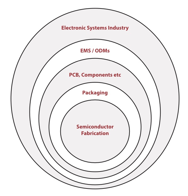
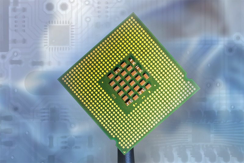
If we start from outside-in, the electronic systems industry – basically finished products that we can all touch and feel as consumers (like TV’s, smartphones, computers, consumer electronic items etc) - consists of several components. There is plastic and metal casing, power supplies, connectors, printed circuit boards (PCB), active and passive components, chips etc. Most of the electronics are mounted on a PCB – which is akin to the foundation of a house upon which the superstructure is built. The chip itself, or the silicon “wafer”, which contains literally hundreds of individual chips, needs to be sliced and individual chips taken from there. These chips, which are essentially just pieces of silicon, then need to be “packaged”, pins attached to them so that they can get power and signals, and then soldered onto a PCB which is designed for each product.
Thus the entire ecosystem is like an onion – each successive peel represents a different part of the entire complex and multi-faceted electronics ecosystem. Each builds on the previous layer and each adds value to the succeeding layer. And the beauty is that almost each layer is a mini ecosystem of its own. Each has its own innovations and key players. Each adds value.
Now let us focus on the innermost core, which provides the ‘intelligence’ or ‘brains’ to any electronic product. Namely, the Semiconductor chip or Integrated Circuit (IC).
Integrated Circuits (ICs) or semiconductor “chips” are the heart and brains of an electronics product. They are what make a smartphone “smart”, or make a TV into an electronic product that can display images and play sound from a digital signal received over a cable, or from a set-top box. They are ubiquitous and present everywhere – from a simple baby’s rattle (toy) to complex circuits powering aircraft or enabling cars to be driven.
Unlike the process of manufacturing (or ‘fabricating’) an integrated circuit, design of a chip is a game of innovation combined with engineering rigour and using CAD tools with literally hundreds of thousands of man years of design knowledge encapsulated in them. It would be no exaggeration to say that from the way it was designed, to the way it was manufactured, and ultimately to the functionality it enables in the equipment it powers. No wonder then it is called the “brains” of an electronic product. Yet very little is known about the manner in which a chip is designed.
Let us start by defining what a semiconductor chip or Integrated Circuit actually is.
Also known as a microchip, a semiconductor chip or integrated circuit (IC) is a small piece of semiconductor material made of silicon that is used to create a wide range of electronic devices and systems. Semiconductor chips are the foundation of modern electronics and are used in a wide variety of products like computers, cell phones, medical devices, automotive products, industrial products etc.
These IC’s are made by etching small circuits, made up of a variety of electronic components, onto a piece of semiconductor material. The circuits are created using a variety of techniques in which a pattern is etched onto the surface of the semiconductor material using light and a chemical etching process.
Semiconductor chips are made by etching patterns into a thin slice of semiconductor material using photolithography, a process that involves exposing the material to light through a mask or stencil. The patterns are then filled in with various materials, such as conductive metals, to create the various components of the IC. The finished chip is then mounted on a circuit board and connected to other components using tiny wires or metal (copper) traces.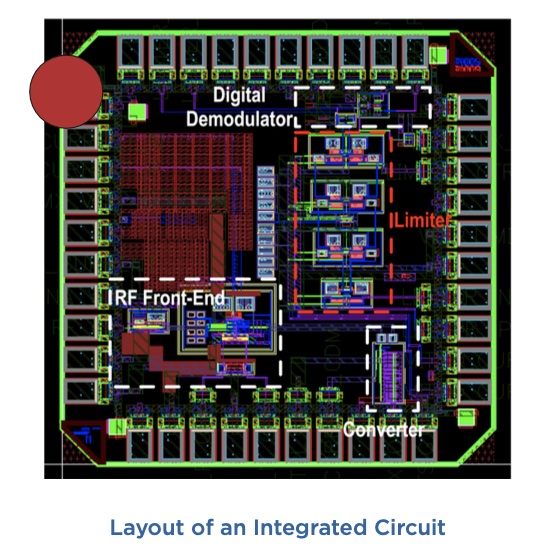
At a top level, the definition of a 4-step process for chip design, as enunciated by Synopsys Inc, a leading Electronic Design Automation (EDA) company, is worth repeating here.
Architectural design of the chip. Wherein the parameters of the chip are determined including its size, desired function, level of power consumption, and preferred cost.
Logic and circuit design. After the parameters are outlined, engineers begin translating the required functions into circuit logic. Today, this process is done on automated logic simulators to verify that everything is in order before production.
Physical design phase. Here, the circuit logic is mapped onto a silicon wafer. Essentially, this is a plan of where each transistor, diode, or other component will sit on the chip.
Verification and sign-off phases are used to verify whether the designed chip is manufacture-able or not, and whether it can withstand the stresses and performance requirements of its assigned function. Specifically, added resistance from wiring, signal crosstalk, and variability are all factors to be considered.
Designing a semiconductor chip like say the flagship Snapdragon processor (from Qualcomm) that powers a lot of smartphones, or a chip like the Intel i7 microprocessor, requires a combination of technical expertise, problem- solving skills, and the ability to work effectively in a multi-disciplinary team setting. Apart from a good grasp of technical skills, these are very complex development projects with many hundreds, even thousands of man years of development effort.
The actual process of designing a semiconductor chip involves several steps and can be quite complex. Since this is a very intense process requiring many highly skilled and qualified engineers, plus the use of very expensive and complex EDA tools, and usually also has several IP blocks being licensed and integrated, the process is expensive, rigorous and heavily monitored by professionally trained project managers. It is not uncommon to have several millions of dollars in costs spent in this complex process of conceiving and designing a chip.
Below, I try and give a simplified overview of the main steps involved in designing a chip:
1. Determine the desired functionality: The first step in designing a semiconductor chip is to define the desired functionality and performance requirements in as much detail as possible. This includes deciding on the specific circuits and components that will be included on the chip, as well as the required input/output and communication interfaces. The definition of functionality will also involve selection of various Intellectual Property (IP) blocks wherein specific functionality (eg USB or BlueTooth or WiFi connectivity, DRAM memory caches etc) are added from previously available sources. (A little later, we will examine factors to keep in mind while selecting IP blocks.). Choices of the processor to be used (a RISC processor from say ARM, or an x86 series CISC processor etc), the bus to be used, the instruction set architecture (ISA) – all of these vital choices have to be made even before the project team is formed. Many times this is dictated by the set of customers or application area, and sometimes (very rarely) this is also dictated by the constraints of the production facilities available.
2. Create a circuit design: Once the desired functionality has been defined, the next step is to create a detailed circuit design. This typically involves using computer- aided design tools (known as EDA tools) to draw the circuit diagram, and to simulate and test the design to ensure that it meets the required specifications. A lot of time is spent in verifying the circuit design using verification tools which have rigorous rules coded into them. Based on the functionality and the application context, additional use-case specific test suites are also designed and run – for instance a SoC with similar architecture (but perhaps different peripherals) could be made for both say a telecom infra and a consumer electronics application. But the test plan and test suites would be very different for the two chips.
3. Create a layout: The next step is to create a layout of the chip, which defines the physical placement and interconnection of the various components and circuits on the chip. This is typically done using specialized layout tools and software.
4. Fabricate the chip: Once the chip design and layout are complete, the next step is to fabricate the chip. First a process called “tape out” is done to set the files to the (typically) commercial semiconductor foundry which will actually fabricate the chip. Consider this as the equivalent of taking the manuscript of a book after the page layout process is complete, and sending to the printer who will mass print the book using say offset printing technology. Fabricating a chip involves multiple stages. It starts with creating a photolithography mask, which is used to transfer the pattern of the chip layout onto a silicon wafer. The wafer is then subjected to various processing steps, such as doping and etching, to create the desired patterns and structures.
5. Test and verify the (finished) chip: After the chip has been fabricated, it must be tested to ensure that it functions correctly and meets the required specifications. This typically involves using specialized equipment to perform a variety of tests on the chip. If any defects are found, the chip design may need to be revised and the process repeated.
It is not uncommon for a reasonably complex semiconductor design project to cost around USD 10-20 million BEFORE it is taped out for fabrication. This is why there is so much emphasis on testing and verification at each and every stage, since the cost of failure is catastrophic. Remember that (unlike software), once a chip is fabricated and (god forbid!) there is a mistake, then it is pretty much useless. Since it is hardware, a “patch” cannot be applied later on to correct it. Hence the emphasis on “first-time-right” for the silicon when it is finally manufactured.
The selection of intellectual property (IP) blocks for a chip is crucial element of the chip design process, as it determines the capabilities and functionality of the chip. There are several factors that should be considered when choosing the IP blocks for a chip.
A top level view of the factors include:
Performance requirements: The desired performance characteristics of the chip, such as operating speed, power consumption, and memory size, will influence the choice of IP blocks. For instance, if the design calls for ultra low power functionality (for IoT applications for example), then the choice of the IP blocks will be very different from say for a chip that will be used in a server type application where 24x7 availability of power is a given. Similarly, mobile devices will need to tradeoff power and performance since high-performance almost always means that power consumption will be higher – thus adversely impacting battery life. Ultimately, the System Architect weighs the power-performance tradeoffs very carefully when selecting the critical IP blocks (processor, memory, connectivity etc).
Compatibility with other components: The IP blocks must be compatible with other components of the chip, such as the process technology and the on-chip interconnects. There is also the issue of whether or not the IP block is “silicon-proven” – i.e. whether or not it has already been integrated into some other chip and has gone through the foundry process and there is working silicon using that IP block. Needless to say, the confidence level in using a silicon-proven IP is significantly higher than one which has only simulation results to show.
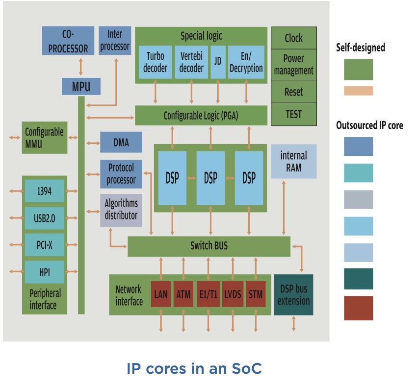
A System on Chip (SoC) is a type of IC that integrates all of the components of a computer or electronic system into a single chip. Hence the term “System” on chip. At a top level these elements are compute, memory, I/O and power management In an SoC, these components comprise of a micro-processor, memory (RAM), input/output interfaces (eg USB, PCI-Express etc), and other digital and analog components.
Designing and manufacturing a SoC is a complex process that involves several stages, from initial concept and design to fabrication and testing. Let us explore the key steps involved in designing and manufacturing a SoC, including the tools and techniques used at each stage.
We have examined these at a high level earlier, but it is worth running over the steps as we look at the realization of a design process into an actual implementation – and not as an abstract process flow.
The first step in designing a SoC is to create a detailed specification of the chip's functionality and performance requirements. This specification will include information on the chip's power consumption, clock speed, input/ output interfaces, and other key parameters. The design team will also need to consider the physical constraints of the chip, such as its size and the materials that will be used to fabricate it.
Once the specification has been developed, the second step is to create a detailed architecture for the SoC.
The architecture will also define the memory hierarchy of the chip and the different types of memory that will be used, such as SRAM, DRAM, and flash memory. The architecture will also define the power domains and power management strategy of the SoC. This is a vital part since a wrongly architected SoC can break the intended functionality of the end product. As an example, if we are designing an SoC for say a portable mobile device working off batteries, then it is logical that there should be fairly aggressive power management techniques available for the System Architect to conserve power and extend battery life. For a memory and compute intensive application, very fast memory and caching will be needed, else the other parts of the system would be waiting for the processor to complete its operations and give them data.
After the architecture is defined, the next step is to design the individual components of the SoC. This can include the microprocessor, memory, input/output interfaces, and other digital and analog components. The design team will use specialized software tools to create a detailed layout of each component, which will then be used to generate the mask data that will be used to fabricate the chip. Many of these components are typically hardened IP blocks which can either be reused, or purchased from specialized vendors. The criteria for selection of IP blocks has already been dealt with earlier in this article.
Once the design of the individual components is complete, the next step is to integrate them into a single chip. This process is known as “physical design” or ‘physical integration’ and involves combining the individual layouts into a single layout that represents the entire SoC. The physical integration process includes the definition of the interconnects between the different components and the power and ground distribution networks. Physical design begins with a Netlist which describes all the components of the SoC and how they connect. Then floor planning takes places where placement of each element is decided keeping in mind factors such as area restrictions, speed, constraints of each component, electrical levels, interconnect lengths etc. Then clock tree synthesis is done inserting buffers or inverters such that the clock is evenly distributed to ensure minimization of latency and skew. The output is GDSII which is a database binary format which is then sent to a foundry for manufacturing the VLSI chip and very detail oriented. Sophisticated EDA tools ensure that complex design rules are kept followed as these steps are done.
Once the physical design is complete, the next step is to prepare the mask data for fabrication. This process involves converting the design data into a format that can be used to create the photomasks that will be used to transfer the design onto the semiconductor wafer. The mask data is also verified to ensure that it is accurate and free of errors.
This step is also called Mask Data Preparation (MDP) or “layout post processing”. The data from the GDSII file is used to do this.
The next step is to fabricate the SoC. This process involves using the mask data to transfer the design onto a semiconductor wafer, which is then cut into individual chips. The wafer is first coated with a layer of photoresist, which is then exposed to light through the photomasks, creating a pattern of the SoC design on the wafer. The wafer is then etched, using the pattern as a guide, to remove the unwanted material and create the individual components of the SoC.
Semiconductor devices are manufactured in Foundries (or ‘Fabs’). These have ultra-clean areas called clean rooms where temperature and humidity are controlled and filters installed to ensure that even microscopic dust particles cannot enter. All technicians working inside the clean rooms wear specialized clothing and pass through high-speed air baths to ensure that all outside particles are removed from their bodies and cannot contaminate the process.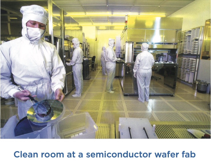
Chip fabrication is an intensely precise and repetitive process whereby alternately metal and silicon are deposited. At each stage, the wafer is cleaned using pure gases or ultra-pure water (UPW) before the next stage of processing starts.
A typically reasonably complex 14 or 7 nanometer wafer can take between 11-15 weeks of processing and can involve around 300 discrete processing steps and 11 or more metal layers.
The clean rooms are hermetically sealed and the wafers move in sealed containers called FOUPS (Front opening universal pods) which move in automated overhead material transporters. Typically the machinery as well as the FOUPS are in a hermetically sealed nitrogen atmosphere to ensure non-degradation of the wafer as it undergoes processing.
A typical wafer is made of extremely pure silicon grown into mono-crystalline cylindrical ingots with a diameter of 300 mm. The ingot is sliced to extract a single wafer of 0.75mm thickness and then polished to obtain a regular and flat surface.
The process of processing of the wafer can be divided into four distinct categories – Deposition, Removal, Patterning and Modification of electrical properties.
Deposition refers to the process of ‘coating or transferring material onto the wafer.
Removal is the process by which the excess coating is removed
Patterning is the shaping or altering of the deposited coating through lithography
Modification of electrical properties refers to the doping of the material already coated to source transistor sources and drains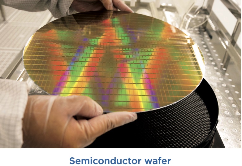
After fabrication, the SoC is tested to ensure that it is functioning correctly. This testing can include both functional testing, to ensure that the chip is performing as expected, and parametric testing, to ensure that the chip's performance is within the specifications. Any defects that are found during testing can be repaired by adding additional transistors or other components to the design.
Foundries employ electronic chip testers which probe each discrete die (individual chips) on a single wafer. Remember that a single wafer can contain several individual chips, which are then cut and packaged – covered later. So the objective of wafer-level testing is to identify the good defect free chips from each wafer. Individual dies which fail the electrical testing are marked with a drop of dye, so that they do not go into the expensive after-process called ATMP.
A very important metric here is “yield” – or the number of good chips from a single wafer. This is typically expressed as a percentage since the number of dies-per-wafer (DPW) varies from design to design. A complex and large footprint chip like say the Pentium will have lesser number of dies per 300 mm wafer, than say a simpler chip like an ADC or DAC. A low yield is expensive for both the foundry and the customer (the company that commissioned the chips). The foundry will be contractually bound to deliver a certain number of working chips to customers. Similarly a company using the foundry to fabricate their chips will need more wafers to get the desired number of chips if the yield is low.
After the fabrication process is completed and the full manufactured die has passed electrical testing, it is sent for packaging. This process is called ATMP (Assembly Test, Marking and Packaging). Some foundries do it themselves, or send the dies to specialized firms which do it. In the latter case, this process is also called OSAT (Outsourced Semiconductor Assembly and Test).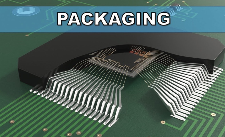
In the packaging process, each individual die is sliced or cut from the mother wafer, then it has pins (bond wired) added to it, and is packaged into a metal/glass/ceramic or plastic casing. For larger and more power-intensive chips, sometimes a heat dissipation metal layer is also added for more efficient dissipation of heat. The pins are used to connect the chip to the circuits on the PCB and the metal, glass or plastic package serves the important function of protecting the die from environmental factors – contamination, pollution, shock etc.
Packaging has evolved constantly and today there are various types of packaging available. As SoC’s become more and more complex, 3-D stacking of wafers within a single package have also come in. There are various standards for packaging – like JEDECEIAJ, Pro Electron etc.
Photolithography
Photolithography or “optical lithography” is the process by which light is used to etch patterns on the substrate of the silicon wafer to translate the VLSI design into an actual circuit. Typically ultraviolet light is used to etch these patterns. When exposed to this UV light, the substrate either breaks down or hardens. The pattern is etched onto the substrate and the residue washed away using solvents. The light used can be normal UV, deep UV or extreme UV or even x-ray. The wavelength of the light determins the minimum feature size that can be etched onto the photoresist material.
A single iteration of photolithography combines several sequential steps.As we have already explained earlier, automated wafer transportation systems carry the wafers from one stage to another. First step is cleaning where organic or inorganic contaminants (eg residue from a previous process) are removed – usually by a wet chemical treatment. After this, the wafer is prepared by heating it to a temperature sufficient to drive off any moisture present on the wafer – typically 150 degree C for about ten minutes. After this, the wafer is prepared for photoresist application by spin coating and the wafer is uniformly coated with photoresist chemical. The spin coating ensures uniform application of the photoresist. After this, the wafer is pre-baked to drive off excess solvents. After this the wafer is then exposed to a pattern of intense light.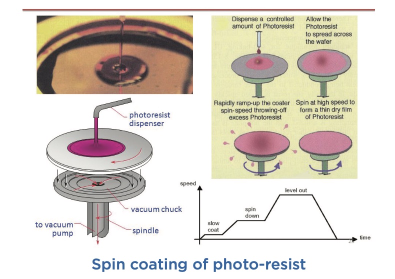
Etch and Ion implantation
After the lithography process is completed, the wafer is cleaned to removed the degraded photoresist and then baked to reveal the 3D channels through which the circuits will be created. There are two types of etch – dry and wet. In dry etching, ultra pure gases are used to defined the exposed pattern on the wafer. Wet etching used chemical baths to wash the wafer. Since chips are made up on multiple layers, it is extremely important to not damage underlying layers as multiple rounds of processing takes place. If for example an etcing process is being done to create a cavity (through hole), then it is extremely important that the hole be made to the precise nano-metric precision, else the next layer will be affected. When you consider that some 3D NAND flash chips now have upto 175 layers, one can only imagine the precision of each step of etching.
After etching is completed, the process of Ion implantation is carried out on the wafer. It is the process by which the wafer is bombarded with either negative or positive ions to tune the electrical conducting properties of the pattern etched onto the wafer. The raw silicon, from which the wafer is made, is neither a perfect insulator or conductor of electricity. Directing electrically charged ions into the structure of the silicon allows the flow of electricity to be controlled and creation of “transistors” to be done. After this, the remaining parts of the photoresist material are removed.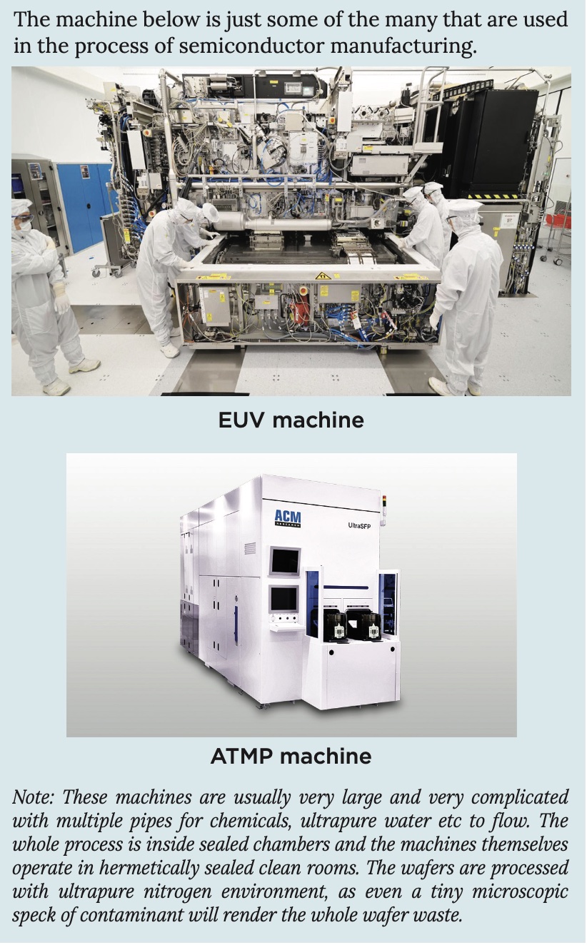
Assembly, Test, Mark & Package (ATMP)
After the processing of the wafer is completed, the individual dies are cut from the wafer, wire-bonding happens and the die is then packaged to create a single chip. The slicing and dicing of the wafer is done using a diamond saw. The individual die is then placed onto a substrate and wires or “pins” attached. The signals form the chip travel to the other parts of the system via these pins which are soldered onto the PCB.
Building a Fab
A semiconductor fabrication factory (“Fab” or foundry) is a continuous process chemical factory. It is very large (50 plus acres of land) and has several additional facilities which work in close cooperation with it.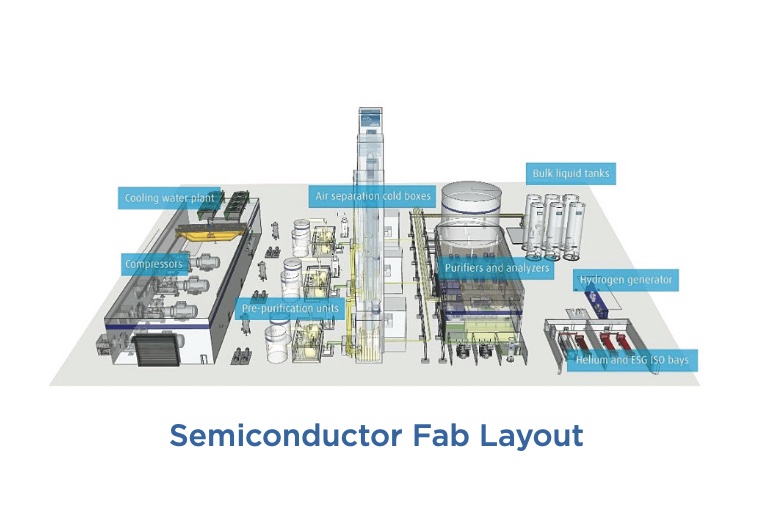
First is effluent treatment. Fabs use what is called ultra- pure water – that too a LOT of it. A typical 300 mm digital fab of 40,000 wafer starts a month will require around 20-25 million litres per day of soft water. The fresh water coming into the plant needs to undergo several stages of purification before it is fit to be used in the process. For semiconductor fabrication, what is needed is ultra pure water (UPW) which is several times cleaner than the distilled water we out into the batteries of our cars. The output also is extremely polluted and needs to undergo several stages of purification before it is evaporated. A fab can typically easily recycle about 75-85 percent of its water. Going beyond that percentage needs investment into sophisticated purification equipment, huge amount of electricity etc.
Second element of the Fab ecosystem is pure gases and their treatment filters. Semiconductor manufacturing requires high-purity gases like Nitrogen, Oxygen, Argon, Hydrogen and Helium. These are used at various stages of wafer processing and are typically washed off the surface of the wafer using UPW. During effluent processing, many of these are extracted from the filters and recycled.
Third is HVAC (Heating, Ventilation and Air conditioning). The process and clean rooms need to be maintained in a very clean state with controlled temperature and humidity. There is very sophisticated HVAC systems that are setup and used in semiconductor foundries – one can safely say that this is an order of complexity and sophistication not easily found/ There are specialized vendors with specialized equipment which can cater to a Semiconductor Fab’s HVAC requirements.
Fourth is clean power that is needed. As per a McKinsey & Co report, a typical medium sized Fab would need roughly the same energy that around 50,000 homes would need per year. Again there are several technologies being used to make semiconductor fabrication more sustainable from the energy and water consumption point of view.
Fifth and most important is the huge investment needed. A typical 28 nm 300 mm fab with 40K wafer starts a month (wsm) could cost around USD 8 billion (roughly Rs 65,000 crores). It needs very expensive and complicated machines with very long lead times to manufacture and deliver. It needs highly skilled and experienced technicians to operate.
As we can see, building a semiconductor fab is a game for the experienced corporations with the ability to raise huge amounts of capital, possess a huge appetite for risk, have deep reservoirs of technical talent and a large number of experienced project management professionals to manage the complex supply chain. Building a fab means investing into the future of technology. This is an investment which will take years, perhaps even more than a decade, to become profitable.
Each has an important part to play and only together can this become a reality. One must remember that Semiconductor is an industry that can only be described as a “technology infrastructure” industry. Therefore, a semiconductor Wafer Fab must be treated as a National Technology Infrastructure Asset (NTIA) and approached only from that perspective. Just as India has approached Space and Atomic Energy as National Missions, with organizations which operate with pan-ministry mandates, so too an NTIA like a Semiconductor Fab must be governed and enabled by a National Electronics Mission (NEM) with a pan-ministry or whole-of-government mandate.
Semiconductors represent the cutting edge of innovation and engineering excellence. It is at the confluence of Innovation, geopolitical pressures, debates around sustainability and resourceallocation. It also needs heavy investment in R&D. Fabs harness technology and engineering excellence to realize the vision, and is perhaps the ultimate aspirational technology goal for a nation.
The semiconductor industry represents technological excellence at various levels. At the design level, it gives enormous opportunities for young digital design engineers to work with cutting-edge tools to develop products for tomorrow. For software experts, the semiconductor and electronics industry creates platforms through which huge mass scale problems can be solved, as these sectors creates the platforms through which the services can be delivered. For material scientists, the field of semiconductor fabrication throws up enormous challenges and scope for pushing the envelope by developing technologies which can promote sustainable manufacturing. For people in areas like HVAC or effluent treatment, their skills and innovation can help this sector reduce costs and promote sustainability. Even for logistics companies, construction firms etc, the design, construction and operation of a Fab throws up multiple opportunities.
As you would have hopefully seen by now dear reader, the semiconductor industry is one where you are only constrained by your imagination – as the industry demands constant innovation, rigorous engineering and project management of a very high order. ©