The continued miniaturization of devices in the nanoscale regime, and the capability to manipulate the matter at these dimensions is expected to revolutionize the future systems for computation, storage and perception in the next few decades. Nanotechnology is not just a natural evolution of the miniaturization trend from sub-100 micrometer scale to sub-100 nanometer scale. The emergence of quantum effects at nanoscale, with a significant departure from the continuum approximation of physical, chemical and biological processes, brings in exciting new possibilities with nanotechnology. In the next few decades, we will go beyond the conventional charge based, digital Silicon CMOS technology, and incorporate several emerging technologies that exploit nanoscale phenomena, to realize extremely powerful machines for high performance computation with augmented perception, mimicking the human brain and sensory organs.
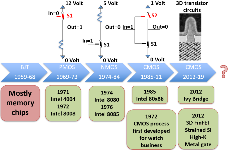
Figure 1 depicts the key milestones in the evolution of compute engines. The bulky and power hungry vacuum tubes used in one of the early digital computers, ENIAC, resulted in rudimentary computation capabilities with the computer weighing 30 tons and consuming 200 kW power. This was certainly not a scalable technology. The invention of semiconductor transistor in 1947 was an inflexion point in the history of miniaturization. This was followed by the invention of the first integrated circuit (IC), a decade later in 1958. However, most of the early ICs were only memory chips and the community was concerned as to what one would do with all those storage devices. Then, the first microprocessor IC invented in 1971, changed the landscape completely. The Intel 4004, a 4 bit microprocessor was realized on 10 μmμm PMOS technology, with a chip size of 12 mm2mm2 and power consumption of 1W. This was soon followed by migration to NMOS technology (Intel 8080 in 1974) and CMOS technology (Intel 80386 in 1985). As exemplified by the famous Moore’s law, the miniaturization trend has continued with CMOS technology scaling, resulting in a new generation of manufacturing technology introduced every 2 to 3 years. This technology scaling, coupled with several innovations in system and circuit architectures, has fuelled the growth of more and more powerful compute engines over the years. For instance, in 2013, the CMOS technology went through another big change with the introduction of 3 dimensional (3D) FinFETs, departing from the conventional planar MOSFETs (Figure 2). By this time, the CMOS technology was also enabled by innovations in nanomaterials technology such as strained Silicon-Germanium channel, HfO2HfO2 high-k gate dielectric with atomically engineered interface. On the architectural front, the introduction of multi-core processors, brought in an unprecedented computing capabilities, even to the hand held devices.
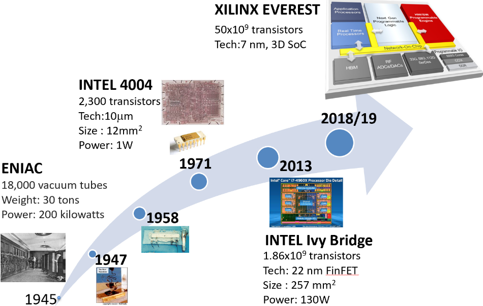
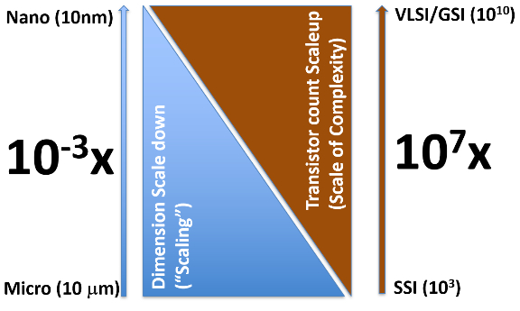
The Everest chip from XILINX, on 7nm CMOS technology with 3D System on Chip fabric, packs 50 billion transistors on single chip, illustrating an amazing technological achievement. It should be recognized that in conjunction to miniaturization, the integration of exponentially large number of transistors is primarily responsible for today’s high performance compute and storage chips. As shown in Figure 3, over the last 5 decades, while the “feature size” of transistors has scaled down by 3 orders of magnitude (10−3)(10−3), the number of components on chip has been increased by 7 orders of magnitude (107)(107). In conjunction with migration from microtechnology to nanotechnology, we have also moved from Small Scale Integration (SSI) to Very Large Scale Integration (VLSI) or Giga Scale Integration (GSI).
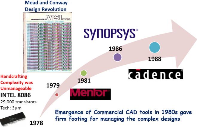
In addition to the underlying nanoscale CMOS technology and ever evolving system and circuit architecture, the highly complex and powerful chips of today owe it to another key enabler, namely the Electronics Design Automation (EDA) using Computer Aided Design (CAD) tools. It is not hard to appreciate that the designing of giga scale integrated circuits would be impossible without sophisticated CAD tools. In late 70s, the handcrafting of the transistors on a chip, turned out to be unmanageable. This led to the emergence of hierarchical abstraction of various components of the chip at behavioural, structural, functional and physical level. The design concepts put forth by Mead and Convey, eventually led to commercial CAD tools to assist in the design of complex chips. Today there is an interesting symbiosis: the advanced CAD tools enabling advanced chips, which in turn enable advanced compute engines that are capable of supporting further advances in CAD tools. The CAD tools have matured so much that the design of a complex chip is akin to writing a software code, through hardware description languages such as Verilog and VHDL. Through the accurate modelling abstraction at different levels, it is possible to achieve first pass success, from specification to the fabrication of a chip, through logic synthesis and layout synthesis tools (Figure 4). For any other emerging nanotechnology option to be successful, it is extremely important to have similar CAD tools to manage complex designs.
With CMOS technology entering the sub-10nm regime, fundamental road blocks are appearing with respect to the underlying materials/process technology and device physics. The big question haunting us quite often is “whether Moore’s law is hitting a red brick wall”? This conundrum can be solved only through some fundamental breakthroughs in nanotechnology in the future. In this context, the guidelines of International Technology Roadmap for Semiconductors (Figure 5), are very instructive.
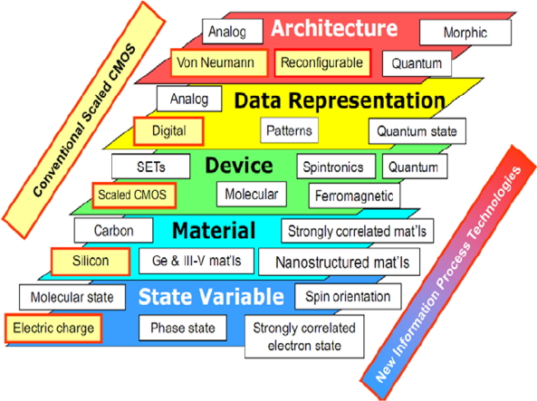
The current compute and storage technologies use “electric charge” as state variable, with “silicon” as the de-facto material, “scaled CMOS” as the device for “digital” data representaion under “von Neumann” computation architecture. At each of these hierarchical levels, multiple other approaches are possible. For instance, the state variable could exploit “spin” of the electrons to build spintronic devices. Alternately, the state variable could be “strongly correlated electronic state”, to build quantum electronic devices, leading to quantum computation architectures. In terms of material choices, we may also go beyond silicon, exploring materials such as carbon, compound semiconductors, 2-dimensional (2D) layered materials such as Transition Metal Dichalcogenides (TMDs) or some other nanostructured materials to realize alternate state variable, device and data representation. All these areas have been very active research topics over the last few years. However, it would still be a very long way to go, in achieving any meaningful manufacturable technology with these alternative options. It should also be highlighted that each of the emerging technology has its own niche, as illustrated on the 4 dimensions of cost, switching time, size and energy. So it is very instructive to appreciate that one size does not fit all, and other technologies might continue to complement and augment the silicon CMOS technology in niche applications.
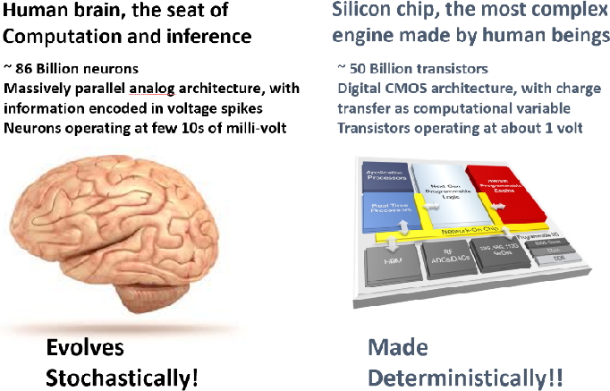
On one hand the number of transistors on a chip (∼50∼50 billion) is approaching the number of neurons in the brain (∼80∼80 billion), thus bringing in the excitement of creating computation chips in the next few decades, mimicking the perception functions of the brain. On the other hand, the on-chip power dissipation due to these large number of transistors has skyrocketed in the range of few 100 watts. Hence the typical power consumption of a state of the art supercomputer, consisting of several racks of microprocessor chips, is in the range of a few mega-W (>106>106 Watts). In contrast, human brain which can beat some of the best supercomputers, in functions such as perception and pattern recognition, consumes a mere 20 W power. This is fundamentally due to two important differences. In terms of operating voltage for the basic building blocks, the transistor operates at about 1V, while the neuron operates at few 10s of milli-V. In terms of architecture, the compute engines use digital architecture, with information coded in charge, while human brain adopts massively parallel analog architecture, with information coded in voltage spikes. Thus the realization of truly brain inspired compute engine is one of the holy grail for the future.
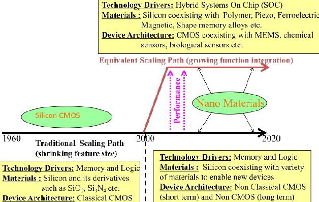
We have so far focussed on the computation and storage applications, which employ traditional dimensional/feature scaling (Figure 7). In the last couple of decades, a new wave of functional scaling has emerged to realize hybrid systems on chips (hybrid SoCs), consisting of sensors and actuators along with the computation and storage elements. It is important to recognize that the miniaturization of electronic chips has been driven by the emergence of new system driver, almost every decade as shown in Figure 7.
For instance, during the last two decades, mobile devices and sensor networks have been the system drivers, enabling large number of wireless chips and sensor chips. The notion of “ambient intelligence” has now emerged due to the possibility of integrating a variety of sensors such as inertial sensors, chemical sensors, biological sensors, along with high perfromance computation and storage engines. The next couple of decades would perhaps witness very powerful artificial intelligence (AI) and machine learning (ML) hardware chips, enabled by the integration of new compute and storage technologies co-existing with a variety of sensors. This could really open up the new era of “perceptive machines”. The next couple of decades are likely to unfold a lot more revolutionary possibilities through nanotechnology.